Skip to content

Tag: Advanced process

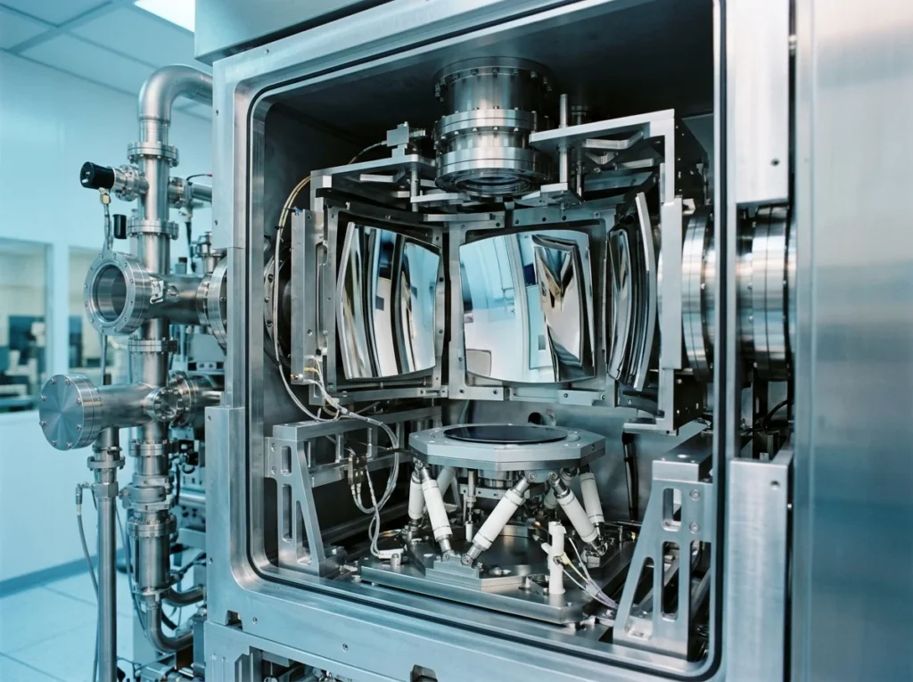
半導體無塵室環境中 ASML 極紫外光微影系統真空反射鏡組與晶圓曝光載台特寫

What is NA numerical aperture? A key analysis of lithography and advanced processes from the optical diffraction limit to High-NA EUV.

Numerical aperture (NA) determines the diffraction limit and wafer resolution in lithography. This article provides an in-depth analysis of ASML, comparing DUV to 0.55 High-NA EUV specifications using the Rayleigh criterion.
Read more
無塵室工程師檢視矽晶圓,背景為不同世代的半導體生產設備

Where are advanced and mature process technologies used? A comprehensive guide from AI chips and automotive MCUs to power devices.

Advanced manufacturing processes do not necessarily outperform mature processes in every aspect. This article analyzes the performance, cost, and reliability of different nodes in AI chips, mobile processors, automotive MCUs, sensors, analog ICs, and power components.
Read more