Skip to content

Category: Industrial Knowledge

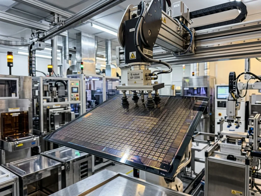
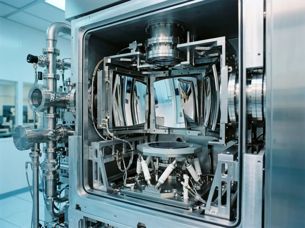
半導體無塵室環境中 ASML 極紫外光微影系統真空反射鏡組與晶圓曝光載台特寫

What is NA numerical aperture? A key analysis of lithography and advanced processes from the optical diffraction limit to High-NA EUV.

Numerical aperture (NA) determines the diffraction limit and wafer resolution in lithography. This article provides an in-depth analysis of ASML, comparing DUV to 0.55 High-NA EUV specifications using the Rayleigh criterion.
Read more
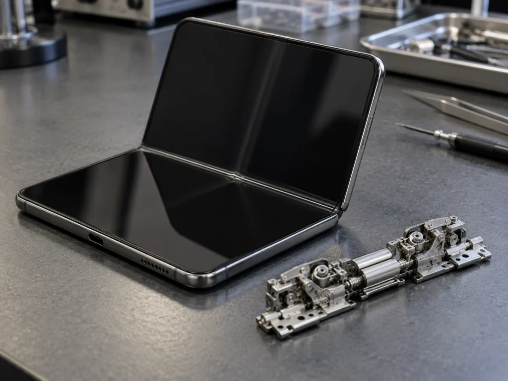
半開的無品牌折疊手機內螢幕與中央折線特寫,旁邊擺放拆出的微型金屬鉸鏈

Why do foldable screens crack? Analysis of UTG bending stress and hinge tolerance failure.

The cracking of folding screens is related to the bending radius of the UTG, the neutral layer, and local contact stress. This paper calculates the bending stress using 30–50 µm glass and analyzes the tolerances of multi-link hinges, metal particles, and drop effects.
Read more
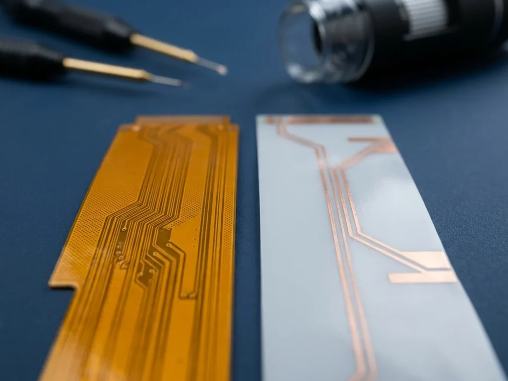
電子實驗室工作台上高頻軟性電路板特寫,對比呈現金黃色 LCP 基板與乳白色 PTFE 複合基板微帶線結構

What are the differences between PTFE and LCP flexible circuit board substrates? A comparison table of Dk/Df dielectric loss, processing difficulty, and high-frequency transmission selection.

What are the differences between PTFE and LCP flexible circuit board substrates? This article provides an in-depth analysis of PTFE, LCP, and MPI in 10GHz applications, particularly relevant to AI servers and 5G millimeter-wave high-frequency transmission.
Read more
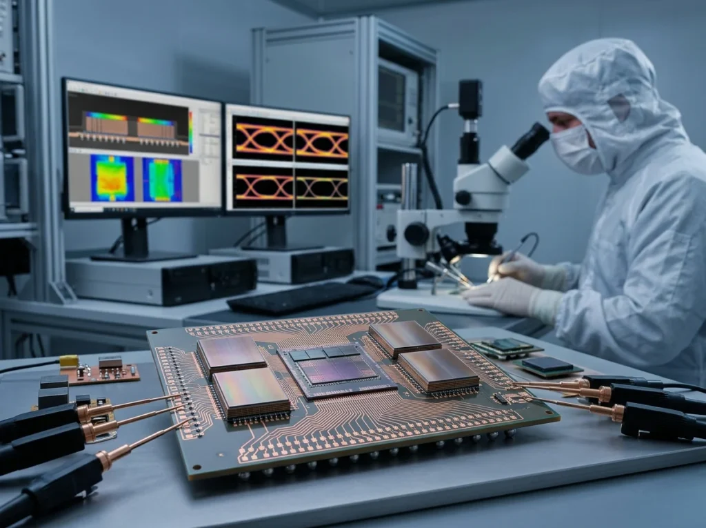
工程實驗室中進行高密度晶片封裝、SerDes 眼圖量測與 AI 加速器模組測試的寫實場景

Why did Nvidia form a major alliance with MediaTek? A technical breakdown from customized ASICs and advanced packaging to chip interconnect architecture.

Nvidia's investment in MediaTek's overseas convertible bonds is more than just a financial investment. This article deciphers the chip engineering architecture: analyzing cloud-based custom ASICs and NVLink Fusion interconnects.
Read more