Skip to content

Tag: Advanced Packaging

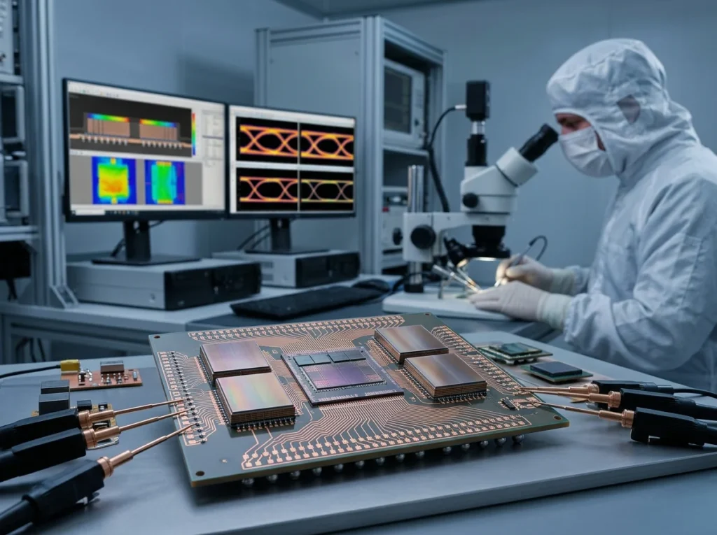
工程實驗室中進行高密度晶片封裝、SerDes 眼圖量測與 AI 加速器模組測試的寫實場景

Why did Nvidia form a major alliance with MediaTek? A technical breakdown from customized ASICs and advanced packaging to chip interconnect architecture.

Nvidia's investment in MediaTek's overseas convertible bonds is more than just a financial investment. This article deciphers the chip engineering architecture: analyzing cloud-based custom ASICs and NVLink Fusion interconnects.
Read more
無塵室工程師在檢查平台上觀察透明玻璃基板與多顆晶片封裝模組

What are the differences between glass substrates and ABF carriers? Analysis of the flatness and warpage challenges in the advanced packaging TGV process.

Why is advanced packaging shifting from ABF organic substrates to glass substrates? This article compares the coefficients of thermal expansion (CTE), flatness, and TGV glass via yield challenges of silicon interlayers, ABF, and glass substrates.
Read more
資料中心交換器內的中央晶片與周圍光引擎連接多條光纖

What is CPO? How can co-packaged optics overcome the transmission bottleneck in AI data centers?

CPO (Commonly Packaged Optics) moves the optical engine next to the switch chip, shortening the high-speed signal path. This article analyzes its operating principle, its differences from pluggable optical modules, its applications in AI data centers, and its heat dissipation and maintenance.
Read more
台灣AI供應鏈全景、Taiwan AI supply chain panorama

Who's selling the shovels in the AI gold mine? The position of Taiwanese supply chains in the AI wave.

Taiwan's role in the AI supply chain extends beyond chip manufacturing; it also encompasses advanced packaging, substrate materials, server rack cooling, and power upgrades. This article uses a relatable perspective to analyze bottlenecks and trends, helping you understand "capacity expansion," "liquid cooling," and more.
Read more