Skip to content

Author: Chris

一個水冷系統 a water cooling system

How to Choose the Right Water Cooling Plate? Understanding 5 Key Water Cooling Plate Designs

In water-cooling systems, the "water-cooled plate" is undoubtedly a core component. As a bridge between the heat source and the coolant, the design of the water-cooled plate directly affects the heat dissipation efficiency and reliability of the entire system. Therefore, understanding water cooling is crucial.
Read more
雲母基板與薄膜示意、Mica substrate with thin film

Flexible semiconductor substrate? Muscovite

When people talk about semiconductor materials, silicon, gallium arsenide, or gallium nitride usually come to mind; few would think of a common mineral: muscovite. However, recent research has linked muscovite with…
Read more
超穎透鏡奈米結構特寫、Close-up of metalens nanostructures

The next generation of lens technology? The birth of the Super Lens.

When we take a photo with our phone, put on VR glasses, or see LiDAR scanning in a car, we are actually dealing with "lenses." Over the past century, lenses have evolved from single-element spherical lenses to multi-element lenses in order to correct aberrations.
Read more
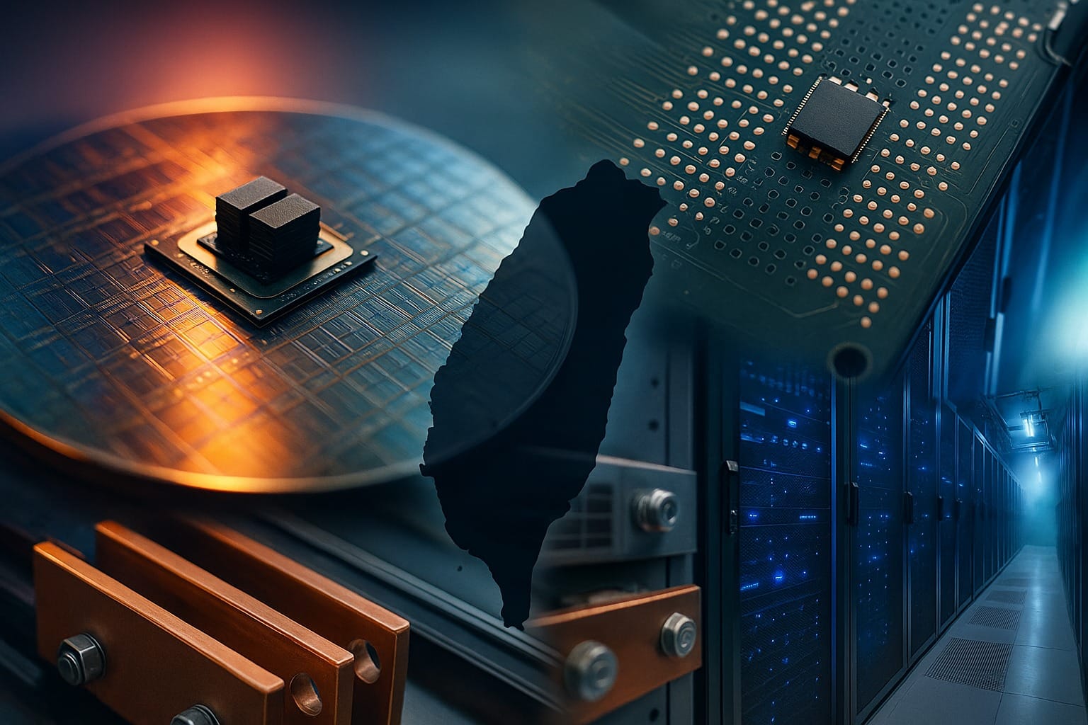
台灣AI供應鏈全景、Taiwan AI supply chain panorama

Who's selling the shovels in the AI gold mine? The position of Taiwanese supply chains in the AI wave.

Taiwan's role in the AI supply chain extends beyond chip manufacturing; it also encompasses advanced packaging, substrate materials, server rack cooling, and power upgrades. This article uses a relatable perspective to analyze bottlenecks and trends, helping you understand "capacity expansion," "liquid cooling," and more.
Read more
Wooden pencils with graphite core, carbon fiber fabric and battery anode roll on desk,鉛筆石墨與碳材料演進意象

Why aren't pencil leads made of lead? The evolution from graphite materials to modern carbon technology.

Pencil lead is actually graphite! Starting with a 16th-century naming misunderstanding, this article analyzes the sp² honeycomb structure of graphite, the 0.335 nm interlayer density and π electron conductivity, explaining that HB/2B hardness is determined by the clay ratio, and further...
Read more
MEMS actuators on silicon die: comb drive, micromirror, microvalve, microgripper 微機電致動器與感測元件、矽晶片特寫

MEMS (Micro-Electro-Mechanical Systems) Manufacturing Process Analysis: From Silicon Wafer to Sensor

A complete guide to MEMS manufacturing processes, from silicon wafers to sensors: lithography, thin film deposition, DRIE deep etching, anodic bonding, vacuum packaging, and calibration testing—easy for beginners to understand. Further master the key processes.
Read more