Table of Content
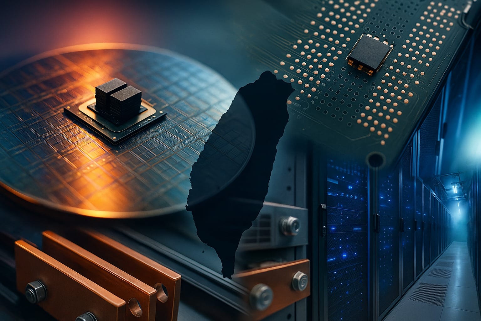
Precision positioning platforms play a crucial role in the semiconductor industry and wafer manufacturing process. With the advancement of nanometer-scale processes, the demands for positional accuracy in exposure machines, wafer inspection equipment, and packaging and testing systems are becoming increasingly stringent. While traditional motor-driven mechanisms can provide a wide range of movement, they fall short in achieving sub-micron or even nanometer-level precision positioning. Piezoelectric ceramics, as materials exhibiting the inverse piezoelectric effect, can directly convert voltage signals into extremely minute mechanical displacements, and are therefore widely used in precision positioning platforms. This article will delve into the working principles of piezoelectric ceramics, their application examples in the semiconductor wafer industry, and their design considerations and future development.
The basic principle of piezoelectric ceramics
The core characteristic of piezoelectric ceramics stems from the piezoelectric effect: when mechanical stress is applied, charge separation occurs, and when an electric field is applied, mechanical deformation is induced. This bidirectional conversion property makes it an ideal material for electrically controlled micro-displacement components. Taking the commonly used PZT (zirconate lead titanate) as an example, its deformation is linearly related to the applied voltage, and the displacement is typically in the micrometer to submicrometer range. Further structural design (such as multilayer stacked designs) can achieve even greater displacement ranges.
Mathematically, the piezoelectric effect can be expressed by the following formula:
$$ S = d_{ij} \cdot E $$in,
- S represents strain.
- dij is the piezoelectric constant (unit: m/V).
- E represents the applied electric field.
If expressed in terms of displacement ΔL:
$$ \Delta L = d_{ij} \cdot V \cdot L $$Where V is the applied voltage and L is the thickness of the piezoelectric ceramic. This means that as long as the voltage input is precisely controlled, stable and predictable micro-displacements can be obtained.
Want to learn about Galinstan, TIM, thermal conductivity, heat dissipation, and liquid metal?
Further Reading :How popular is liquid metal in heat dissipation applications? Let's look at the truth from the perspective of thermal conductivity.
Application of piezoelectric ceramics in semiconductor precision positioning platforms
In semiconductor wafer manufacturing, lithography machines (steppers/scanners) need to precisely align the exposure pattern with the wafer surface, with alignment accuracy typically required to be less than 10 nanometers. Traditional ball screws or linear motors are no longer sufficient for this requirement, while piezoelectric ceramic-driven nanoscale positioning platforms can effectively compensate for this need.
Typical applications include:
- Wafer alignmentNanoscale position correction in the XY plane is achieved through piezoelectric actuators to ensure the overlap accuracy between the photomask and the wafer.
- Focal length controlPiezoelectric ceramics are used for nanoscale adjustment in the Z-axis direction to maintain the optimal depth of focus during photolithography.
- Detection and Measurement PlatformElectron microscopes (SEMs) or optical inspection equipment rely on piezoelectric platforms to achieve submicron scanning.
- Packaging and bondingPiezoelectric actuators control the micro-displacement of the chip and the substrate, ensuring precise alignment of the solder joints.
Based on actual data, a typical PZT stacked piezoelectric actuator can achieve a resolution of 0.1 nanometers and a response time of less than 1 millisecond, far superior to traditional mechanical drives. This makes it an indispensable core component in semiconductor devices.
Design Considerations and Challenges
Although piezoelectric ceramics have the advantages of high precision and high-speed response, the following points should still be noted in their application:
- Nonlinearity and hysteresis effectPiezoelectric ceramics exhibit hysteresis under high voltage, resulting in incomplete reversibility of displacement. To solve this problem, it is usually necessary to combine closed-loop control with position sensors (such as capacitive or optical sensors).
- Temperature sensitivityThe piezoelectric constant dijd_{ij}dij changes with temperature and needs to be corrected through environmental control or material compensation in semiconductor cleanrooms.
- Travel restrictionsPiezoelectric displacement is typically only a few tens of micrometers, so it is often paired with a mechanical amplification structure (flexure hinge) to expand the range of motion.
- Drive voltage requirementsTraditional single-layer ceramics require hundreds of volts, while multilayer structures can reduce this to tens of volts, but still require a dedicated drive power supply.
Future Development and Trends
As wafer fabrication processes advance towards the 2-nanometer node, piezoelectric ceramics will play an even more crucial role in precision positioning platforms. Next-generation materials such as lead-free piezoelectric ceramics (e.g., KNN: potassium sodium niobate) are gradually replacing lead-containing PZT, complying with environmental regulations. On the other hand, piezoelectric thin films (such as AlN and ZnO) are being integrated into MEMS devices, promising applications in wafer-level sensing and micro-actuators.
Furthermore, artificial intelligence and real-time control technologies are being integrated with piezoelectric positioning platforms, enabling compensation algorithms to automatically correct nonlinear behavior and further improve accuracy. Future precision positioning platforms will not only be passive mechanisms but also active systems with intelligent sensing and adaptive control.
Want to learn about ball screws, roller screws, precision transmissions, screw life, and preload rigidity?
Further Reading :How to Choose Between Ball Screws and Roller Screws? Three Key Indicators: Lifespan, Efficiency, and Preload
Conclusion
Piezoelectric ceramics, with their nanometer-level displacement characteristics driven by voltage, have become core components of precision positioning platforms in semiconductor manufacturing. In critical stages of wafer fabrication, such as photolithography, alignment, inspection, and packaging, piezoelectric actuators demonstrate irreplaceable advantages. Although challenges such as nonlinearity, temperature sensitivity, and stroke limitations exist, these problems are gradually being overcome through advanced material design, closed-loop control, and intelligent algorithms. Looking ahead, piezoelectric ceramics will continue to drive precision manufacturing in the semiconductor industry, laying the foundation for breakthroughs in wafer technology.