Table of Content
In the field of digital photography and image processing, CMOS (Complementary Metal-Oxide-Semiconductor) and CCD (Charge-Coupled Device) are two major image sensing technologies. Both are used to convert light into digital signals, but they differ significantly in their working principles, performance characteristics, and application scenarios. This article will introduce these two core products of image processing: CMOS and CCD.
Basic principles of CMOS and CCD
CMOS (Complementary Metal-Oxide-Semiconductor)
Each pixel of a CMOS sensor contains a set of photodiodes and amplifier circuitry, allowing light signals to be processed directly at the pixel layer and manufactured using standard semiconductor processes. This enables CMOS sensors to operate with low power consumption and high-speed readout.
1. Low power consumption: Because each pixel can process signals independently, there is no need to transfer charge line by line during reading, which can effectively reduce power consumption.
2. High-speed processing: It can read multiple pixels at the same time, making it suitable for high-speed photography and real-time image processing.
3. Lower cost: Compatible with general semiconductor manufacturing processes, and the manufacturing cost is lower than that of CCD.
4. High noise: Because each pixel has an internal amplification circuit, it is prone to generating fixed pattern noise.
5. Slightly lower light-sensing efficiency: The readout circuit within the pixel occupies part of the light-sensing area, resulting in a lower fill rate.
CCD - Charge-Coupled Device
CCD sensors do not have built-in amplifier circuits in their pixel array. Instead, they use charge transfer to transfer the accumulated charge of each pixel row by row to the sensing area, and then the amplifier reads and outputs the charge. This method ensures lower signal interference, resulting in higher quality images.
1. Higher image quality: Because the signals of all pixels are processed by a unified amplifier, the uniformity and signal-to-noise ratio of the image are better.
2. Higher light-sensing efficiency: Unlike CMOS, it does not have built-in circuits to block incident light, so the utilization rate of the light-sensing area is higher.
3. High power consumption: The charge transfer method consumes more energy, especially in high-resolution sensors.
4. Slower read speed: Because the charge must be transferred to the output line by line, the read speed cannot be as fast as CMOS.
Comparison from various aspects
The following is a comparison of CMOS and CCD in various aspects:
| characteristic | CMOS | CCD |
|---|---|---|
| Manufacturing costs | 低 | 高 |
| Power consumption | 低 | 高 |
| Image quality | Slightly low (more noise) | High (low noise) |
| Read speed | 高 | 低 |
| Sensitivity | Low (due to filler ratio) | 高 |
| Application areas | Mobile phones, monitors, consumer cameras | Scientific research, advanced photography, medical imaging |
Application scenarios of CMOS and CCD
CMOS sensors are widely used in smartphones, network cameras (such as surveillance cameras and dashcams), consumer digital cameras, drones and action cameras (such as GoPro), and automotive image sensing (such as cameras in autonomous vehicles) due to their low power consumption, high speed readout, and low cost.
Due to their advantages of high image quality, low noise, and high sensitivity, CCD sensors still hold a place in the following fields: astrophotography (such as the Hubble Space Telescope), medical imaging (such as X-ray sensors), industrial inspection (such as precision measuring equipment), and professional photography (such as high-end digital cameras and movie cameras).
Want to learn about optical lenses, lens components, and related industries?
Further Reading :Optical Lens Industry Analysis - Composition and Manufacturing of Lens Modules
CMOS manufacturing principle
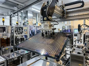
The manufacturing process of CMOS image sensors is the same as that of standard CMOS semiconductor processes (such as logic chips, microprocessors, etc.), mainly using planar processes and photolithography to manufacture chips.
Each pixel of a CMOS sensor contains:
- Photodiode: Responsible for sensing light and generating electric charge.
- Amplifier: Each pixel has an independent amplifier circuit that can immediately convert charge into a voltage signal.
- Readout Circuit: Composed of MOS transistors, it is responsible for controlling signal reading.
- Analog-to-Digital Converter (ADC): Converts optical signals into digital signals, and is usually integrated into a chip.
CMOS pixel design typically uses "Active Pixel Sensor (APS)," meaning that each pixel has an active element that can independently read data, thus enabling high-speed reading and reducing power consumption.
CMOS manufacturing steps
1. Silicon substrate preparation: Use high-purity silicon wafers (usually 8-inch or 12-inch).
2. Photolithography: Using exposure technology to etch sensor circuits.
3. Ion Implantation: Controlling charge conduction regions, such as P-type and N-type regions, through doping techniques.
4. Metallization: Establishing CMOS circuitry, including readout circuitry and digital signal processing.
5. Sensing area and microlens: Microlenses are added to improve light collection efficiency (back-illuminated CMOS BSI technology).
6. Packaging: Finally, the wafer is cut and packaged into a sensing module.
Benefiting from the evolution of standard semiconductor manufacturing processes, CMOS has now developed technologies such as the following:
- Backside Illumination (BSI): Improves light-sensing efficiency.
- Stacked CMOS: Reduces signal interference and improves image quality.
- Global Shutter CMOS: Improves the rolling shutter effect in moving images.
CCD manufacturing principle
The manufacturing process of CCD image sensors differs from that of standard CMOS. CCDs require specialized manufacturing techniques, primarily using high-quality silicon to enhance light sensitivity.
CMOS and CCD sensors differ in their image imaging principles, optical requirements, and light-sensing characteristics, which affects lens selection when paired with a lens module. Key influencing factors include sensor structure, light sensitivity, noise processing, and image requirements.
A CCD consists of a series of light-sensing pixel arrays and charge transport channels, and its structure includes:
- Photosensitive area: Uses a PN junction to convert photons into electrical charges.
- Charge-coupled channel (CCC): Charge is gradually transferred to the readout end through voltage control.
- Output Amplifier: Converts the last accumulated charge into an image signal.
Unlike CMOS, CCD does not have a separate pixel amplifier. Instead, it reads images in a concentrated manner through "line-by-line transfer", resulting in purer image quality.
CCD manufacturing steps
1. Silicon substrate preparation: High-quality silicon wafers are used, which are usually of higher purity than those used in CMOS.
2. Photolithography and Doping: Forming photosensitive areas and charge transport channels.
3. Oxidation & Dielectric Layer: Establish an insulating layer for efficient charge transfer to reduce dark current.
4. Electrode Deposition: Creating a control gate for charge transfer.
5. Output Node: Establishes a unified signal reading mechanism to reduce noise.
6. Packaging & AR Coating: An anti-reflective coating is used to improve light utilization.
CCD manufacturing technology has seen the following developments:
- Full-Frame CCD: Used for astrophotography, offering the highest image quality.
- Interline CCD: Offers faster image readout speeds and is suitable for high-end cameras.
- Back-illuminated CCD (BI-CCD): Improves light sensitivity and is used in scientific photography.
Differences in lens module selection between CMOS and CCD
Light-sensing characteristics and lens selection
CMOS sensors have a lower fill rate (because each pixel has a built-in amplification circuit, occupying a portion of the photosensitive area). Therefore, the optical design of the lens requires higher precision, including the following:
- High light transmittance (for lenses with low F-numbers) is used to compensate for lower light sensitivity.
- Wide-angle lenses (less than 50mm) are commonly used in mobile phone and surveillance photography.
- It is suitable for pairing with aspherical lenses to reduce aberrations.
CCDs, due to their higher fill factor and stronger light sensitivity, perform better in low-light conditions. They can be paired with lenses with higher F-numbers (F2.8 – F4 and above) because the sensor itself is more sensitive to light. They are often used in telephoto and high-precision lenses, such as: astrophotography (requiring high-quality telephoto lenses) and medical imaging (requiring high-resolution lenses).
Spectral response and lens coating
Different sensors have varying sensitivities to the spectrum, which affects the selection of lens coatings.
- CMOS sensors are sensitive to infrared (IR) light, so they are usually paired with IR cut filters to avoid color distortion in images.
- CCDs are more sensitive to ultraviolet (UV) and blue light, so they need to be paired with lenses with anti-UV coatings to reduce color shift.
- Surveillance cameras often have IR cut filters in their CMOS lens modules to prevent nighttime images from appearing reddish.
- Scientific photography (such as microscopic imaging) may use full-spectrum lenses in conjunction with the sensitivity of CCDs.
Resolution and Lens Selection
Modern CMOS sensors offer increasingly higher resolutions (such as 4K, 8K, and even higher), which places stricter demands on lens resolution. High-resolution CMOS sensors (such as 48MP and 100MP) require high-MTF lenses to ensure that image quality is not limited by insufficient lens resolution. CCDs, on the other hand, generally have lower resolution but stronger light sensitivity, making them suitable for high-quality images in low-light environments, such as night vision photography and astrophotography.
Example of resolution and lens matching:
| Sensor resolution | Lens requirements |
|---|---|
| 8MP CMOS | Standard consumer lenses |
| 48MP CMOS | Low aberration, high resolution lens |
| 200MP CMOS | Ultra-high resolution lenses, such as high-end lenses from Zeiss and Leica. |
| 2MP CCD | Suitable for lenses with an aperture of F4 or higher, such as astrophotography lenses. |
| 10MP CCD | Higher resolution optical lenses are required, such as lenses specifically designed for microscopic imaging. |
Shutter mode and lens application
CCD sensors are mostly global shutters, meaning all pixels are exposed simultaneously, making them suitable for high-speed photography and industrial inspection, and they do not exhibit rolling shutter effect.
CMOS sensors mostly use rolling shutters, which are prone to distortion when moving at high speeds. Therefore, they need to be paired with lenses with fast shutter speeds or use global shutter CMOS sensors.
There are indeed differences in lens selection between CMOS and CCD sensors. Key influencing factors include: light sensitivity, resolution, shutter speed, and application scenario. In summary,
- CMOS sensors require lenses with low F-numbers and high light transmittance, making them particularly suitable for high-speed image processing and the consumer market.
- CCDs have high light sensitivity and are suitable for high-quality lenses with high F-numbers, making them suitable for professional photography, medical imaging, and astrophotography.
- High-resolution CMOS (such as 100MP) requires high MTF optical lenses to avoid image blurring or insufficient resolution.